Clock signal
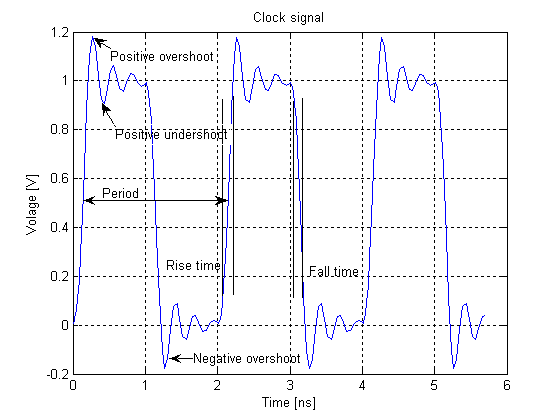
In electronics and especially synchronous digital circuits, a clock signal (historically also known as logic beat)[1] is an electronic logic signal (voltage or current) which oscillates between a high and a low state at a constant frequency and is used like a metronome to synchronize actions of digital circuits. In a synchronous logic circuit, the most common type of digital circuit, the clock signal is applied to all storage devices, flip-flops and latches, and causes them all to change state simultaneously, preventing race conditions.
A clock signal is produced by an electronic oscillator called a clock generator. The most common clock signal is in the form of a square wave with a 50% duty cycle. Circuits using the clock signal for synchronization may become active at either the rising edge, falling edge, or, in the case of double data rate, both in the rising and in the falling edges of the clock cycle.
Other circuits[edit]
Some sensitive mixed-signal circuits, such as precision analog-to-digital converters, use sine waves rather than square waves as their clock signals, because square waves contain high-frequency harmonics that can interfere with the analog circuitry and cause noise. Such sine wave clocks are often differential signals, because this type of signal has twice the slew rate, and therefore half the timing uncertainty, of a single-ended signal with the same voltage range. Differential signals radiate less strongly than a single line. Alternatively, a single line shielded by power and ground lines can be used.
In CMOS circuits, gate capacitances are charged and discharged continually. A capacitor does not dissipate energy, but energy is wasted in the driving transistors. In reversible computing, inductors can be used to store this energy and reduce the energy loss, but they tend to be quite large. Alternatively, using a sine wave clock, CMOS transmission gates and energy-saving techniques, the power requirements can be reduced.
Distribution[edit]
The most effective way to get the clock signal to every part of a chip that needs it, with the lowest skew, is a metal grid. In a large microprocessor, the power used to drive the clock signal can be over 30% of the total power used by the entire chip. The whole structure with the gates at the ends and all amplifiers in between have to be loaded and unloaded every cycle.[10][11] To save energy, clock gating temporarily shuts off part of the tree.
The clock distribution network (or clock tree, when this network forms a tree such as an H-tree) distributes the clock signal(s) from a common point to all the elements that need it. Since this function is vital to the operation of a synchronous system, much attention has been given to the characteristics of these clock signals and the electrical networks used in their distribution. Clock signals are often regarded as simple control signals; however, these signals have some very special characteristics and attributes.
Clock signals are typically loaded with the greatest fanout and operate at the highest speeds of any signal within the synchronous system. Since the data signals are provided with a temporal reference by the clock signals, the clock waveforms must be particularly clean and sharp. Furthermore, these clock signals are particularly affected by technology scaling (see Moore's law), in that long global interconnect lines become significantly more resistive as line dimensions are decreased. This increased line resistance is one of the primary reasons for the increasing significance of clock distribution on synchronous performance. Finally, the control of any differences and uncertainty in the arrival times of
the clock signals can severely limit the maximum performance of the entire system and create catastrophic race conditions in which an incorrect data signal may latch within a register.
Most synchronous digital systems consist of cascaded banks of sequential registers with combinational logic between each set of registers. The functional requirements of the digital system are satisfied by the logic stages. Each logic stage introduces delay that affects timing performance, and the timing performance of the digital design can be evaluated relative to the timing requirements by a timing analysis. Often special consideration must be made to meet the timing requirements. For example, the global performance and local timing requirements may be satisfied by the careful insertion of pipeline registers into equally spaced time windows to satisfy critical worst-case timing constraints. The proper design of the clock distribution network helps ensure that critical timing requirements are satisfied and that no race conditions exist (see also clock skew).
The delay components that make up a general synchronous system are composed of the following three individual subsystems: the memory storage elements, the logic elements, and the clocking circuitry and distribution network.
Novel structures are currently under development to ameliorate these issues and provide effective solutions. Important areas of research include resonant clocking techniques ("resonant clock mesh"),[12][13][14][15]
on-chip optical interconnect, and local synchronization methodologies.
Adapted from Eby Friedman Archived 2014-08-12 at the Wayback Machine's column in the ACM SIGDA e-newsletter by Igor Markov
Original text is available at https://web.archive.org/web/20100711135550/http://www.sigda.org/newsletter/2005/eNews_051201.html