Katana VentraIP

Surface-mount technology

Surface-mount technology (SMT), originally called planar mounting,[1] is a method in which the electrical components are mounted directly onto the surface of a printed circuit board (PCB).[2] An electrical component mounted in this manner is referred to as a surface-mount device (SMD). In industry, this approach has largely replaced the through-hole technology construction method of fitting components, in large part because SMT allows for increased manufacturing automation which reduces cost and improves quality.[3] It also allows for more components to fit on a given area of substrate. Both technologies can be used on the same board, with the through-hole technology often used for components not suitable for surface mounting such as large transformers and heat-sinked power semiconductors.

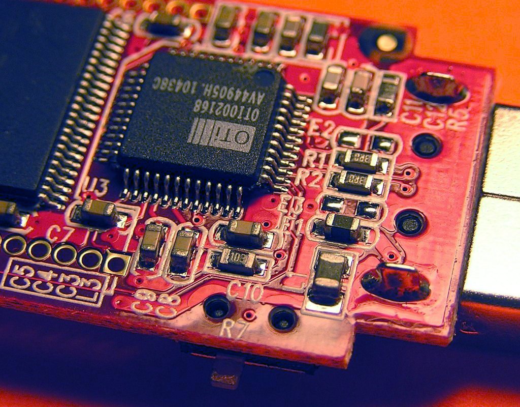
An SMT component is usually smaller than its through-hole counterpart because it has either smaller leads or no leads at all. It may have short pins or leads of various styles, flat contacts, a matrix of solder balls (BGAs), or terminations on the body of the component.

History[edit]

Surface-mount technology was developed in the 1960s. By 1986 surface mounted components accounted for 10% of the market at most, but was rapidly gaining popularity.[4] By the late 1990s, the great majority of high-tech electronic printed circuit assemblies were dominated by surface mount devices. Much of the pioneering work in this technology was done by IBM. The design approach first demonstrated by IBM in 1960 in a small-scale computer was later applied in the Launch Vehicle Digital Computer used in the Instrument Unit that guided all Saturn IB and Saturn V vehicles.[5] Components were mechanically redesigned to have small metal tabs or end caps that could be directly soldered to the surface of the PCB. Components became much smaller and component placement on both sides of a board became far more common with surface mounting than through-hole mounting, allowing much higher circuit densities and smaller circuit boards and, in turn, machines or subassemblies containing the boards.


Often the surface tension of the solder is enough to hold the parts to the board; in rare cases parts on the bottom or "second" side of the board may be secured with a dot of adhesive to keep components from dropping off inside reflow ovens if the part is above the limit of 30g per square inch of pad area.[6] Adhesive is sometimes used to hold SMT components on the bottom side of a board if a wave soldering process is used to solder both SMT and through-hole components simultaneously. Alternatively, SMT and through-hole components can be soldered on the same side of a board without adhesive if the SMT parts are first reflow-soldered, then a selective solder mask is used to prevent the solder holding those parts in place from reflowing and the parts floating away during wave soldering. Surface mounting lends itself well to a high degree of automation, reducing labor cost and greatly increasing production rates.


Conversely, SMT does not lend itself well to manual or low-automation fabrication, which is more economical and faster for one-off prototyping and small-scale production, and this is one reason why many through-hole components are still manufactured. Some SMDs can be soldered with a temperature-controlled manual soldering iron, but unfortunately, those that are very small or have too fine a lead pitch are impossible to manually solder without expensive hot-air solder reflow equipment. SMDs can be one-quarter to one-tenth the size and weight, and one-half to one-quarter the cost of equivalent through-hole parts, but on the other hand, the costs of a certain SMT part and of an equivalent through-hole part may be quite similar, though rarely is the SMT part more expensive.

Smaller components.

Much higher component density (components per unit area) and many more connections per component.

Components can be placed on both sides of the circuit board.

Higher density of connections because holes do not block routing space on inner layers, nor on back-side layers if components are mounted on only one side of the PCB.

Small errors in component placement are corrected automatically as the surface tension of molten solder pulls components into alignment with solder pads. (On the other hand, through-hole components cannot be slightly misaligned, because once the leads are through the holes, the components are fully aligned and cannot move laterally out of alignment.)

Better mechanical performance under shock and vibration conditions (partly due to lower mass, and partly due to less cantilevering)

Lower resistance and inductance at the connection; consequently, fewer unwanted RF signal effects and better and more predictable high-frequency performance.

Better (lower radiated emissions) due to the smaller radiation loop area (because of the smaller package) and the lesser lead inductance.[16]

EMC performance

Fewer holes need to be drilled. (Drilling PCBs is time-consuming and expensive.)

Lower initial cost and time of setting up for mass production, using automated equipment.

Simpler and faster automated assembly. Some placement machines are capable of placing more than 136,000 components per hour.

Many SMT parts cost less than equivalent through-hole parts.

The main advantages of SMT over the older through-hole technique are:[14][15]

SMT may be unsuitable as the sole attachment method for components that are subject to frequent mechanical stress, such as connectors that are used to interface with external devices that are frequently attached and detached.

SMDs' solder connections may be damaged by compounds going through thermal cycling.

potting

Manual prototype assembly or component-level repair is more difficult and requires skilled operators and more expensive tools, due to the small sizes and lead spacings of many SMDs. Handling of small SMT components can be difficult, requiring tweezers, unlike nearly all through-hole components. Whereas through-hole components will stay in place (under gravitational force) once inserted and can be mechanically secured prior to soldering by bending out two leads on the solder side of the board, SMDs are easily moved out of place by a touch of a soldering iron. Without developed skill, when manually soldering or desoldering a component, it is easy to accidentally reflow the solder of an adjacent SMT component and unintentionally displace it, something that is almost impossible to do with through-hole components.

[17]

Many types of SMT component packages cannot be installed in sockets, which provide for easy installation or exchange of components to modify a circuit and easy replacement of failed components. (Virtually all through-hole components can be socketed.)

SMDs cannot be used directly with plug-in (a quick snap-and-play prototyping tool), requiring either a custom PCB for every prototype or the mounting of the SMD upon a pin-leaded carrier. For prototyping around a specific SMD component, a less-expensive breakout board may be used. Additionally, stripboard style protoboards can be used, some of which include pads for standard sized SMD components. For prototyping, "dead bug" breadboarding can be used.[18]

breadboards

Solder joint dimensions in SMT quickly become much smaller as advances are made toward ultra-fine pitch technology. The reliability of solder joints becomes more of a concern, as less and less solder is allowed for each joint. Voiding is a fault commonly associated with solder joints, especially when reflowing a solder paste in the SMT application. The presence of voids can deteriorate the joint strength and eventually lead to joint failure.[20]

[19]

SMDs, usually being smaller than equivalent through-hole components, have less surface area for marking, requiring marked part ID codes or component values to be more cryptic and smaller, often requiring magnification to be read, whereas a larger through-hole component could be read and identified by the unaided eye. This is a disadvantage for prototyping, repair, rework, reverse engineering, and possibly for production set-up.

Melt solder and remove component(s)

Remove residual solder (may be not required for some components)

Print solder paste on PCB, directly or by dispensing or dipping

Place new component and reflow.

Board-to-board connectors

Chip carrier

Electronics

Electronics manufacturing services

List of electronics package dimensions

List of integrated circuit packaging types

Plastic leaded chip carrier

Point-to-point construction

Printed circuit board

RoHS

SMT placement equipment

Through-hole technology

Wire wrap

RKM code